1 Introduction
It is very important to set the interrupt detection point during the real-time analysis of the DSP system by using the integrated development and debugging platform CCS combined with the JTAG-based simulator. The interrupt detection point can interrupt the execution of the program for specific operations, such as It can input and output data files, refresh charts and data windows, etc., and it is more convenient to observe the display results of data processing in real-time analysis.
2. Simulator based on JTAG technology
JTAG technology, or boundary scan technology, is a special electronic system test technology, which is commonly referred to as the IEEE1149.1 standard. It has been widely used in various industries, as shown in Figure 1, a JTAG conforming to the IEEE1149.1 standard. The device, unlike the different logic devices, includes a TAP (Test Access Port) controller internally, and then serializes all of the input and output pins into a single scan link via a scan link inside the chip.
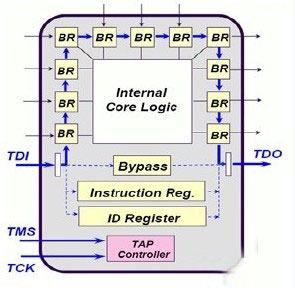
Figure 1 JTAG device
The boundary scan technology based on the IEEE1149.1 standard is first applied to the DFT technology of large-scale integrated circuits and system-on-chip design, which not only ensures the logic of the peripheral pin part of the integrated circuit chip, but also the self-embedded inside the chip. Testing mechanisms and the like play a role in integration and control. Secondly, the JTAG interface of the chip can realize the online programming of the integrated circuit chip including FPGA, DSP and processor, and can also realize the online debugging of the chip. The former is to use this mode to realize the design download, and the latter utilizes Virtual online debugging technology is to transfer part of the internal logic information during the running of the chip to the computer for analysis and interpretation through the JTAG interface. Third, the boundary-scanning technology based on the JTAG standard can be applied in the field of connectivity testing of printed circuit boards by connecting the boundary scan chains of JTAG devices together and controlling the appropriate data information to be passed in the scan chain. The output is monitored to identify issues related to printed circuit board connectivity and component functionality.
The JTAG-based emulator is used to simulate the hardware of the chip, such as single-step execution of the program, setting the interrupt detection point, etc. The hardware simulation can be used to understand the detailed operation of the program inside the chip. The JTAG emulator is mainly used to simulate the chip, and the chip can also be programmed through the JTAG interface (write the program to the chip). Its interface mode is LPT (parallel) port, PCI or ISA card, USB port. One end of the JTAG emulator is connected to the PC through the USB port, and the other end is connected to the DSP target board through the JTAG plug. It is recommended to connect the JTAG emulator to the PC first, and then connect to the DSP target board. [8]
3. Signal generator based on TMS320 C54XDSP chip
3.1 TMS320 C54x series DSP chip
The TMS320 C54x family of DSP chips is fabricated using static CMOS technology. The chip uses a modified Harvard architecture to use separate buses for program memory and data memory; it can fetch instructions and operands simultaneously, improving operational efficiency and versatility. Advanced CPU design and hardware logic designed for applications improve chip performance; Designed for rapid follow-up development; high performance and low power for advanced IC processing; highly specialized instruction structure for fast computation and optimization of high-level language operations; single instruction loops and blocks Instruction loop function; block memory move instructions provide better program and data management; instructions with two or three operand read capabilities; instructions that return quickly from interrupts have a variety of on-chip peripherals and memory configuration schemes .
3.2 signal generator
a) Connect the hardware, first power up the DSP target, the indicator light is on.
A CCS operating environment.
a) Create a new project and add relevant documents to the project.
In the Open option of a Project menu, select the compilation project of the signal generator in the pop-up dialog box.
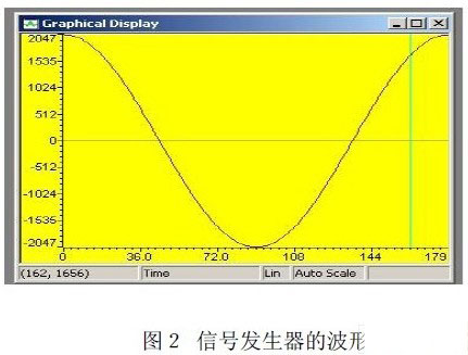
A Rebuild All option in the Project menu, compile and link the project. After no error, select the Load Program option in the File menu, select the *.C file, and load the program. Select the Time/Frequency setting graph property in the graph option in the View menu, select Start Address as dacdata, set the Acquisition Buffer Size to 180, set the Display Data Size to 180, and set the Dsp Data Type to 16-bit signed integer. Click OK to observe the waveform of the signal generator, as shown in Figure 2:
Children School Lunch Box,School Lunch Box,Double Layer Lunch Box,Plastic Lunch Box
Leqishi Plastic Products Co., Ltd. , http://www.plastic-food-containers.com