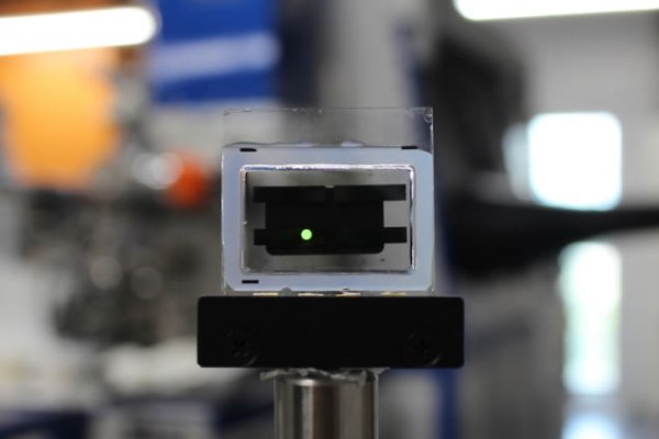
Organic Light Emitting Diode (OLED) test, including thick layer of mixed perovskite to emit green light. Source: Kyushu University William J. Porta Jawaj Jr.
The researchers combined organic thin films with organic-inorganic perovskite transport layers to produce high-performance thick organic light-emitting diodes (OLEDs). This material has the same luminous efficiency as the reference thin oled, and can be used to make inexpensive displays and screens that can emit the same color from all viewing angles.
Oled uses organic molecular layers to effectively convert electricity into light. The organic layer is placed between two electrodes, one of which is usually transparent. They are ideal applications for next-generation displays and lighting, but the problem is that they need to be made as thin as about 100 nanometers. This is because although organic molecules are good luminous bodies, they are usually poor conductors. Only such a thin layer can transmit electricity to the center of the device, the active light-emitting part.
The disadvantage of the thin layer is that it cannot completely cover the defects and residues on the substrate. These defects create a shunt path between the electrodes. The shunt path is a hassle because it is through these that the charge carriers bypass the organic layer without recombination to produce light. In the case of an electrical short circuit, this will lead to inefficient or even complete equipment failure. More importantly, the light reflected between the front and back of the thin layer will produce a cavity effect, which will distort the emission color at a large viewing angle.
Make thick movies
A thicker organic transport layer is a possible solution to this problem, but the thicker the layer, the higher the driving voltage needs to be.
Although researchers have tried to make thick OLEDs with organic single crystals, they cannot be produced on a large scale. They also tried to dope the organic layer chemically to increase the conductivity, but additional light absorption bands appeared in the material, reducing the electroluminescence efficiency.
A research team at Kyushu University in Japan said that they may have found a solution to this problem by using organic-inorganic perovskite lead methylene ammonium chloride (MAPbCl3) instead of organic molecules as the transport layer. In their device, the researchers sandwiched a layer of luminescent molecules commonly used for oled between the perovskite layers. Therefore, they were able to increase the total thickness of the active MAPbCl3 layer to 2000 nanometers, which is more than 10 times the thickness of the standard oled, without the need for high drive voltages.
The surface roughness of these films is also very low, which means that they can better cover the substrate and inhibit the formation of terrible shunt paths. They also do not absorb visible light, which is why they can be used to make thicker oled without affecting the internal electroluminescence quantum efficiency.
Due to the x-ray diffraction pattern and the absorption spectrum of the film, the researchers also confirmed that the film was stable in air even after 11 days. They say another advantage that cannot be ignored is that oled made with these films may be cheaper because they cost less than organic materials.
Overthought for 30 years
So far, researchers have mainly used perovskite as the light emission source. Perovskite has an ABX3 structure, where A is cesium and methylammonium (MA) or formamidine (FA), B is lead or tin, and X is chlorine, Bromine or iodine. This is because, due to their tunable band gap, they can absorb light in a wide range of wavelengths in the solar spectrum. However, in this study, the Japanese research team only used them to transmit electrical energy-they are also good in this respect because carriers can diffuse through them quickly and for a long time-and are reserved for light emission Part of organic molecules. In this way, it can produce thick devices with the same luminous efficiency as the reference thin oled.
Chihaya Adachi, head of the research team, said: "These results overturned the idea that oled was limited to thin films for 30 years and opened a new path for low-cost, reliable and uniform manufacturing of OLED-based displays and lighting." "Based on this Work, perovskite will be regarded as a versatile, high-performance material, not only for oled, but also for other organic electronic devices such as lasers, storage devices and sensors. "
An Infrared Thermometer is a thermometer which infers temperature from a portion of the thermal radiation sometimes called black-body radiation emitted by the object being measured. They are sometimes called laser thermometers as a laser is used to help aim the thermometer, or non-contact thermometers or temperature guns, to describe the device's ability to measure temperature from a distance. By knowing the amount of infrared energy emitted by the object and its emissivity, the object's temperature can often be determined within a certain range of its actual temperature. Infrared thermometers are a subset of devices known as "thermal radiation thermometers".
Forehead Thermometer,Non-Contact Infrared Thermometer,Infrared Thermometer,Smart Baby Thermometer
Dongguan Yibao Technology Co., Ltd. , https://www.yibaomedical.com