Technology Trends Based on InGaN technology and existing manufacturing facilities, strain engineering can provide a viable method for microdisplays. Based on the strain engineering of indium gallium nitride (InGaN) multiple quantum wells, the University of Michigan has developed a monolithically integrated amber-green-blue LED (Figure 1). The strain engineering is achieved by etching nano-pillars of different diameters.
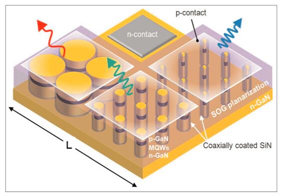
Figure 1. Top-down manufacturing schematic of nano-pillar LED arrays of various diameters
The researchers hope that in the future, red-green-blue LEDs can be produced using 635 nm photoluminescence quantum wells, providing a feasible method for microdisplays based on such pixel LEDs. Other potential applications include lighting, biosensors, and optogenetics.
In addition to the support of the National Science Foundation (NSF), Samsung also provided support for manufacturing and equipment design. Researchers hope to develop chip-level multicolor LED platforms based on existing manufacturing infrastructure.
The epitaxial material was grown on 2 inch unpatterned sapphire by metal organic chemical vapor deposition (MOCVD). The luminescent active area consists of five 2.5 nm InGaN wells separated by a 12 nm GaN gate. The electron blocking layer and the p-contact layer consist of 20 nm aluminum gallium nitride (p-Al 0.2 Ga 0.8 N) and 150 nm p-GaN, respectively.
Electron beam lithography was used to shape the nanopillars, and a mixed wet-dry etching process was performed using a nickel mask. Most of the etching is a dry inductively coupled plasma, the wet etching stage is used to achieve the final diameter, and the damage in the dry etching step is removed. The etching depth is about 300 nm. The etching mask is protected throughout the manufacturing process in order to protect the p-GaN surface.
After plasma-enhanced chemical vapor deposition (PECVD) of 50 nm silicon nitride, the structure was planarized with spin-on glass to electrically isolate the n- and p-GaN portions.
The flattened structure is dry etched back to expose the tip of the column. The nickel mask material was removed with nitric acid solution. The p-contacted nickel/gold metallization is thermally annealed in air.
The electrical performance of the device shows a low leakage of about 3x10⁻⁷A per pixel at 5V reverse bias. Low leakage is attributed to two factors - the flat quantum well provides low current crowding effects, as well as the strain-induced carrier to nanocube center limit. The risk of declining effects due to greater current density in narrower nanopillars can be improved by reducing the strain, thus reducing the quantum confinement that occurs due to the electric field induced by the charge polarization of chemical bonds in III-nitrides. "Stark effect."
The pixels consist of columns with different diameters and emitting different colors (Figure 2). As the diameter increases, the wavelength becomes longer and changes more. The researchers attributed the change to changes in the quantum well thickness on the wafer.
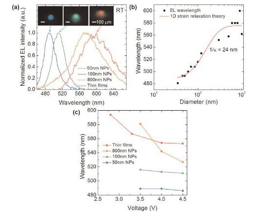
Figure 2. (a) Room-temperature electroluminescence spectra of blue (487 nm), green (512 nm), orange (575 nm), and amber (600 nm) light obtained from 50 nm, 100 nm, and 800 nm diameter nanopillars and thin film LED pixels. .
(b) The wavelength of light obtained by one-dimensional stress relaxation theory.
(c) The location of the main peak at various applied bias voltages.
As the voltage and current injections increase, narrower and narrower nanotubes also show less wavelength blue shift. The blue shift of 800 nm diameter nanocolumn pixels is 40 nm between 2.8V and 4V. This is due to the fact that the research team screens the strain dependent piezoelectric field in the trap.
The team stabilized the output wavelength of the pixel by fixing the bias voltage and changing the intensity by pulse frequency modulation. Through this experiment it was shown that all pixel types give stable wavelengths and relative electroluminescence intensities, which appear almost linearly with the duty cycle of the pulsed signal. The pulse width is 400μs. The pulse frequency varies between 200 Hz and 2000 Hz.
The original title of U.S.-developed monolithic integrated tricolor LED will contain more color combinations in the future
China Built In Gas Oven, Gas Oven ,Gas Stove Oven Supplier
for this kind of goods ,we use good quality stainless steel with high quality GAS STOVE owen .
China Built In GAS OVEN ,Gas Oven supplier & manufacturer, offer low price, high quality Gas Stove Oven,Gas Oven With Stove, etc.
We support like this kind of goods to different coutnry for more than 20 years ,we had good experience .with good quality and competition price .
Built In Gas Oven,Gas Oven,Gas Stove Oven,Gas Oven With Stove
GAS OVEN
Built In Gas Oven,Gas Oven,Gas Stove Oven,Gas Oven With Stove
GUANGZHOU AIJINGSI TRADING LIMITED , https://www.aichugashob.com